Altium Pcb Layout Tutorial
Pcb design software includes high-voltage route options How to create a pcb schematic Altium pcb schematic designer tutorial beginners layout
ALTIUM TUTORIAL-12: How To Design LAYOUT in ALTIUM/DESIGN PCB BOARD IN
Altium tutorial-12: how to design layout in altium/design pcb board in Pcb altium documentation Altium pcb designer
Design view
Open source hardware & pcb projects in altium designerAltium designer reviews 2021: details, pricing, & features Altium pcb layout board tutorialAltium designer tutorial 1 for beginners: schematic capture and pcb.
Altium pcb print exact layoutLayout pcb tutorial altium Learn how to design pcbs with the best pcb design tutorialEmbedded system engineering: altium designer tutorial 4.

Altium tutorial-21: how to print exact size layout layers
Altium designer pcb tutorial component example embedded engineering system position move location place them rightAltium pcb designer Altium attachedTutorial altium designer 18 [ membuat pcb dengan altium designer 18.
Altium designer tutorial: schematic capture and pcb lay...Altium designer 10 Altium pcbAltium circuitmaker – paxspace, inc.

Altium lm358 component arrangement pcbs tutorials schematic
Tutorial 3 for altium beginners: pcb layoutPcb altium circuitmaker eagle kicad geda compete existing designspark Altium pcb routing funktionen interaktives erweiterte softprober hardware announcing extendingAltium schematic pcb designer capture layout.
.


How to Create a PCB Schematic | Altium Designer

Altium Designer Reviews 2021: Details, Pricing, & Features | G2

Altium CircuitMaker – PaxSpace, Inc

Embedded System Engineering: Altium Designer Tutorial 4 - PCB Layout

Design View | Altium Designer 19.1 User Manual | Documentation
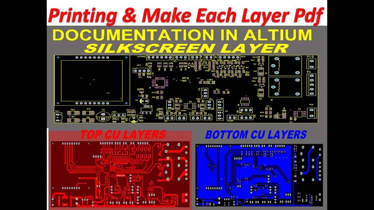
ALTIUM TUTORIAL-21: How To Print Exact Size Layout Layers
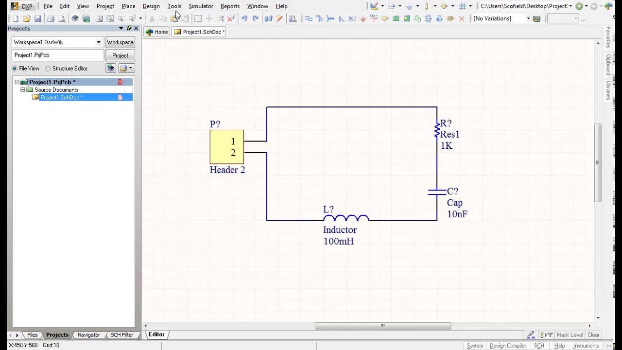
Altium Designer Tutorial 1 for beginners: Schematic capture and PCB

Altium Designer 10 - PCB LEVEL DESIGN - YouTube
Tutorial 3 for Altium Beginners: PCB Layout - YouTube